Schematics and Building the Circuit
A Closer Look at the QTI
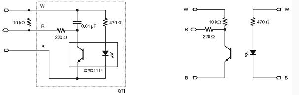
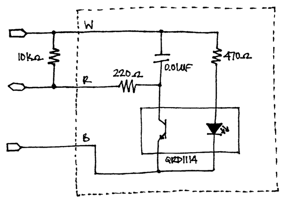
The QTI module is designed for close-proximity infrared (IR) detection. Take a look at the small square black box just above the QTI label, it’s nested below the capacitor and between the two resistors. That’s a QRD1114 reflective-object sensor containing an infrared diode behind its clear window and an infrared transistor behind its black window. When the infrared emitted by the diode reflects off a surface and returns to the black window, it strikes the infrared transistor’s base, causing it to conduct current. The more infrared incident on the transistor’s base, the more current it conducts.
When used as an analog sensor, the QTI can detect shades of gray on paper and distances over a short range if the light in the room remains constant. With this circuit, you can set P3 high and then test it with RCTIME to measure how long it takes the capacitor to discharge through the IR transistor. Since the IR transistor conducts more or less current depending on how much IR it receives, the RCTIME measurement can give you an indication of distance or shade of gray.
If all you want to know is whether a line is black or white, the QTI can also be converted to a digital sensor. This is how the array of four QTI sensors will be used later in our Boe-Bot line following application.
When W is connected to Vdd and B is connected to Vss, the R-terminal’s voltage will drop below 1.4 V when the IR transistor sees infrared reflected from the IR LED. When the IR LED’s signal is mostly absorbed by a black surface, the voltage at R goes above 1.4 V. Since the BASIC Stamp interprets any voltage above 1.4 V as 1 and any voltage below 1.4 V as 0, this circuit shown in Figure 2 gives us a quick and easy way to detect a black line on a white background.
Figure 2 - QTI Circuit
Mounting the QTIs
- Make sure all pieces are present in your kit. If anything is missing, contact Parallax Tech Support.
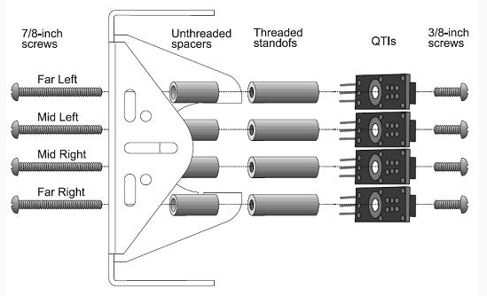
- Referring to Figure 3, insert the 7/8-inch screws through the top of the Boe-Bot chassis, at the three slots near the front. Two screws will go through the center slot, and one screw each in the right and left slots.
- On the underside of the chassis, slip a 1/2-inch unthreaded spacer on each screw, followed by a 1-inch threaded standoff.
- Attach a QTI sensor to the other end of each threaded standoff, using a 3/8-inch screw. The sensors should be facing downwards, and the 3-pin headers on each sensor should be pointing towards the back of the chassis.
- If necessary, slightly loosen the 7/8-inch screws and adjust the position of the QTI sensors so that they are closely positioned edge to edge.
- Tighten all connections securely.
Figure 3 – QTI Mechanical Assembly
QTI Line Follower Circuit
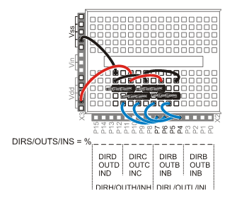
Figure 4 shows the schematic for four QTIs along with a partially completed wiring diagram. Although there are many ways this circuit can be built, the setup shown below is useful because it's thrifty with breadboard real-estate.
Figure 4 - QTI Circuit and Wiring Diagram Part 1
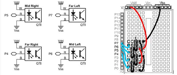
Figure 5 shows how to connect the servo extension cables to the male-male headers that were plugged into the breadboard in Figure 4. The other end of each cable is plugged into a QTI. Be careful when you make these connections, and pay close attention to the wire colors listed in the figure. Notice that the far left and mid left cables have white wires that plug onto header pins in the same breadboard row. The same applies to the mid right and far right QTI cables. Instead of common white wires, the mid left and mid right QTI cables share a pair of black wires.
Figure 5 – QTI Circuit and Wiring Diagram Part 2

The QTI Detection Subroutine
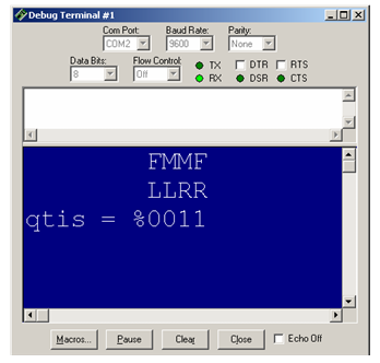
It's a good idea to test all the sensors with the Debug Terminal before taking the Boe-Bot for a spin on the line following course. The next example program (CheckQtiSubroutine.bs2) has a Debug Terminal display you can use to make sure the QTIs are properly discerning the difference between black vinyl electrical tape and white paper. Figure 6 shows what you'd want to see in the Debug Terminal display when the middle-right and far-right QTIs are over black electrical tape, and the other two are over white paper.
Figure 6 - QTI Debug Terminal Test Display
Example Program: CheckQtiSubroutine.bs2
- Affix two 3/4 inches wide pieces of electrical tape to a white sheet of paper, each a few inches long and spaced 3/4 inches apart.
- Use the BASIC Stamp Editor to open and run CheckQtiSubroutine.bs2.
- Place each QTI over the electrical tape and then over the white paper and verify that it detects the difference, 0 for white and 1 for black.
- Verify that the QTIs are connected in the right order and that they are close enough together. As you slide the Boe-Bot slowly across the electrical tape stripe, from right to left, verify that this sequence appears in the Debug Terminal: %0000, %1000, %1100, %0100, %0110, %0010, %0011, %0001, %0000.
- Also try placing all the QTIs over the electrical tape. The qtis variable should display %1111.
Keep your Boe-Bot away from direct sunlight, and avoid direct light from incandescent desk lamps during these tests. Also, keep your line following course away from these sources of infrared interference.
' CheckQtiSubroutine.bs2
' Displays QTI sensor states. 0 means white surface, 1 means black.

' {$STAMP BS2}
' {$PBASIC 2.5}


qtis VAR Nib                  ' qti black/white states

OUTB = %1111                  ' Set OUTB bits to 1

DEBUG CRSRX, 8, "FMMF", CR,   ' Display bit positions
      CRSRX, 8, "LLRR", CR

DO                            ' Main DO...LOOP
  GOSUB Check_Qtis            ' Get QTI states
  DEBUG BIN4 ? qtis, CRSRUP   ' Display QTI states
  PAUSE 100                   ' 1/10 s delay
LOOP

Check_Qtis:
' Result -> qtis variable. 0 means white surface, 1 means black
' surface.

  DIRB = %1111                  ' P7..P4 -> output
  PAUSE 0                       ' Delay = 230 us
  DIRB = %0000                  ' P7..P4 -> input
  PAUSE 0 ' Delay = 230 us
  ' PULSOUT UnusedPin, 0        ' Delays = 208 + (Duration*2) us
  qtis = INB ' Store QTI outputs in INB

  RETURN
If you had problems with two QTIs sensing 1 when only one of them should have, try adjusting the standoffs so that the QTIs are further apart. Not so far that you can get 0000 when the line is between two QTIs though! On the other hand, if only one QTI sensed 1 when the stripe was between two of them, they may need to be positioned closer together. Otherwise, your Boe-Bot is ready for line following!
How CheckQtiSubroutine.bs2 Works
The BASIC Stamp has a variety of parallel I/O control features that make it possible to perform operations on groups of I/O pins. CheckQtiSubroutine.bs2 uses the BASIC Stamp's DIRB and OUTB variables to control the directions and output states of the I/O pins P7, P6, P5, and P4. When these I/O pins are set to input with DIRB = %0000, the program also takes a snapshot of the binary states these I/O pins sense as a result of the four QTIs' R-pin voltages with the command qtis = INB. Before going into detail about how these variables are used in the Check_Qtis subroutine to simultaneously check the four QTIs, let's take a closer look at how the BASIC Stamp's Parallel I/O control variables work.
BASIC Stamp Parallel I/O Control
In addition to the 13 words of variable RAM, the BASIC Stamp has three extra words of memory for controlling the directions of the I/O pins, setting their output states and reading their input states. These word variables don't have to be declared as variables because they already have the following PBASIC keyword names:
- DIRS – Controls I/O pin directions
- OUTS – Controls I/O pin directions
- INS – Monitors I/O pin states
Since each word variable has 16 bits, the DIRS, OUTS, and INS variables conveniently have one bit apiece for each of the BASIC Stamp's 16 I/O pins. Each bit either stores a 1 or a 0, which in turn relates to some I/O pin characteristic, be it I/O pin direction, high/low output state, or sensed input state.
Figure 7 shows how each bit in the DIRS, OUTS, and INS variables maps to the BASIC Stamp's I/O pins. Bit 0 of each variable either controls or senses P0. Bit 1 of each variable controls/senses P1, and so on, all the way up to bit 15, which controls/senses P15.
Figure 7 - I/O pin bit mapping
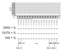
Figure 8 shows some example commands can be used to control as well as read all 16 I/O pins with single commands that write values to and read values from DIRS, OUTS, and INS:
Figure 8 - Register example commands
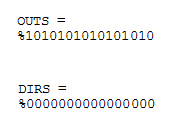
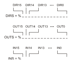
Figure 9 shows how each variable's bits can be individually accessed with bit variables DIR0 through DIR15, OUT0 through OUT15 and IN0 through IN15. Each of these bit variable names are also PBASIC keywords.
Figure 9 - Variable bit access
PBASIC even has variables with keywords for parallel byte and nibble operations (Figure 10). Notice that the DIRB, OUTB, and INB nibble variables used in CheckQtiSubroutine.bs2 map to the BASIC Stamp I/O pins that are connected to the QTIs' R-pins.
Figure 10 - Keywords for byte and nibble operations
Notice how each I/O pin has one bit in the DIRS, OUTS, and INS variables. Collectively, the three bits define the I/O pin's direction, output state (when it's an output) and sense the signal the I/O pin is either sending or receiving. For example, bit-3 of the DIRS variable (DIRS.BIT3 or DIR3) sets the direction of I/O pin P3 to output if it is 1, or input if it is 0. If the direction of P3 is output, bit-3 in the OUTS variable (OUTS.BIT3 or OUT3) makes the I/O pin send a high signal if it's 1 or a low signal if it's 0. If P3 is set to output, bit-3 of the INS variable will store whatever is in bit-3 of the OUTS variable. If P3 is set to input, it will store a 0 if the voltage at P3 is below 1.4 V, or a 1 if the input signal is at or above 1.4 V.
I/O Variable Facts
A bit in the DIRS variable makes an I/O pin an output if it's 1 or an input if it's 0.
As an output an I/O pin will send a high signal if the corresponding bit in the OUTS variable is 1, or a low if that bit is 0.
Bit values in the OUTS variable have no effect on I/O pins that are set to input.
I/O pins that are set to input also have no effect on external circuits; they only sense voltage signals applied by external circuits.
Bit values in the INS variable will match the values in the OUTS variable if the I/O pin is an output. If the I/O pin is an input, the INS bit value depends on the voltage the I/O pin senses (1 if the voltage is at or above 1.4 V, or 0 if it's below that level).
These same rules apply to Byte, Nib, and Bit I/O variables:
DIRH / OUTH / INH and DIRL / OUTL / INL
DIRA / OUTA / INA through DIRD / OUTD / IND
DIR0 / OUT0 / IN0 through DIR15 / OUT15 / IN15
Here is an example of two commands that define a variety of settings, simultaneously, on all sixteen I/O pins with just two commands:
OUTS = %1010101010101010
DIRS = %0000000011111111
OUTS = %1010101010101010 sets and clears alternate bits in the OUTS variable. The leftmost bit is 1, which means P15 will send a high signal, so long as bit 15 in the DIRS variable is 1 (output). The second bit from the far left in the OUTS variable controls the P14 output state, and it's 0, which will make P14 send a low signal. This pattern repeats itself down through bit 0, the rightmost bit, which controls P0.
After setting and clearing alternate bits in the OUTS variable, the command DIRS = %0000000011111111 sets P15 through P8 to input, so they just listen for signals, and won't pay any attention to the OUTS variable. However, the command also sets the bits for P7 through P0 in the DIRS variable to 1’s, making them outputs. Since the OUTS variable has alternating 1’s and 0’s, P7 will send a high (5 V) signal, and P6 will send a low (0 V) signal. P5 also sends a high signal, and so on through P0, which sends a low.
Here, also is an example of using the INS variable to take a snapshot of all the BASIC Stamp I/O pins with just two commands:
DIRS = %0000000000000000
variable = INS
The command DIRS = %0000000000000000, sets all the I/O pins to input. Then, variable = INS takes all the input states sensed by the I/O pins at the instant the command is executed and copies them to variable. Let's say you didn't use the command DIRS = %0000000000000000 before variable = INS.
If DIRS is still %0000000011111111 from the parallel output example, the I/O pins will behave differently. Since bits 15 through 8 in the DIRS variable are all 0, bits 15 through 8 in the INS variable will still store whatever input states the P15 through P8 I/O pins sense. Again, those states depend on the voltages of the devices or circuits connected to those I/O pins. On the other hand, bits 7 through 0 in the DIRS variable are all 1s, so those I/O pins are outputs. As a result, bits 7 through 0 in the INS variable will instead store whatever they sense the I/0 pins are transmitting — a 1 if it's high (5 V), or 0 if it's low (0 V). Let's say again that the values in the OUTS variable are also from the previous example; that's OUTS = %1010101010101010. Because of this, bits 7 through 0 in the INS variable will store %10101010.
PBASIC Commands that Modify DIRS, OUTS, and INS
The DIRS, OUTS and INS variables are automatically updated whenever you use HIGH, LOW, INPUT, OUPUT, TOGGLE, or REVERSE. Let's say you use the command LOW 3. It automatically puts a 0 in bit-3 of the OUTS variable to set up the low signal and 1 in bit-3 of the DIRS variable to make it an output and transmit the signal. HIGH 3 would instead write a 1 to bit-3 in the OUTS variable, along with 1 to bit-3 in the DIRS variable. If you use INPUT 3, it will make the I/O pin an input, which stores a 0 in bit-3 of the DIRS variable.
You can also access the I/O direction, output and input variables as bytes, nibbles or even bits. The byte variable keyword names end in H for P15 through P8 and L for P7 through P0. So, there's DIRH, OUTH, and INH, and there's also DIRL, OUTL, and INL. There are also A, B, C and D I/O nibbles. A is P3 through P0, B is P7 through P4, C is P11 through P8, and D is P15 through P12. So, OUTB = %1101 sets up P7, P6, and P4 to send high signals and P5 to send a low signal. DIRB = %1111 changes all the I/O pins to outputs so that the high/low signals can be sent. Each I/O variable is also bit addressable. For example, DIR15, OUT15 control the direction and output state of P15 while IN15 reads its input. The same applies to for P14 and DIR14, OUT14, and IN14, and so on...
PBASIC Commands that Modify DIRS, OUTS, and INS
The BASIC Stamp Editor's Help documentation also has information about the BASIC Stamp's parallel I/O variables. After clicking Help and selecting Index, type OUTB into the Keyword field. The term OUTB will appear in the index list. When you click it and the Display button, the PBASIC Syntax Guide takes you to an excerpt from the BASIC Stamp Manual on Memory Organization and Variables.
Parallel I/O Control for Monitoring Four QTIs
Going back to the image above showing PBASIC variable keywords (above), the QTIs are connected to P7 through P4, so the parallel I/O operations are performed using DIRB, OUTB, and INB. In the example program, DIRB sets the direction of those four I/O pins, OUTB sets the output states, and INB reads inputs.
At the beginning of the program, the command OUTB = %1111 sets the bits for P7, P6, P5, and P4 so that the I/O pins will all send high signals. Since the BASIC Stamp initializes all I/O pins to input, this command will not have any effect until the corresponding bits in the DIRB variable are set to 1, which happens later in the program. The I/O pins remain inputs, but they are now all ready to send high signals when the DIRB variable bits are set to %1111.
In the Check_Qtis subroutine, P7 through P4 have to be set high to discharge all the QTIs' capacitors. Since the lower plate of each capacitor is connected to the R-pin as shown below, the voltage at the each R-pin rises as each QTI's capacitor discharges. The command that sets P7 through P4 to output is DIRB = %1111, and since all the OUTB bits were set to 1 at the beginning of the program, all the I/O pins send high signals. After all the I/O pins change to output-high, which causes the BASIC Stamp I/O pins to short the QTI's R-pin to the BASIC Stamp's 5 V supply, a brief delay is necessary to let the QTI capacitors discharge. PAUSE 0 inserts a 0.23 ms delay into the BASIC Stamp 2 program to give the QTIs' capacitors enough time to fully discharge.
Figure 11 - QTI Schematic
After DIRB = %1111 and PAUSE 0, the QTIs' capacitors are all just about fully discharged, and the voltage at each R-pin is very close to 5 V. The next step is to set all the I/O pins to input and wait for another 0.23 ms with the commands DIRB = %0000 and PAUSE 0. When all the I/O pins that were output high get changed to input, the QTIs' capacitors start to charge. How quickly they charge is governed by how much infrared the QRD1114's infrared transistor receives. The QTI should be between 1/16 and 3/16 of an inch from a surface. So, the IR light the QRD1114's IR transistor receives should come from the QRD1114's IR emitting diode as it reflects off the surface.
Since white surfaces reflect infrared, more of it gets back to the QRD1114's IR transistor's base, which causes the IR transistor to conduct more current. When the IR transistor conducts more current, the capacitor can charge quickly, which in turn causes the R-pin's voltage to drop below 1.4 V during the 0.23 ms delay caused by the Check_Qtis subroutine's second PAUSE 0 command. If the QTI is over a black surface, very little IR will get back to the transistor's base, which means it won't conduct much current. In that case, the capacitor charges slowly in comparison, and the voltage at the R-pin doesn't make it to 1.4 V during the 230 μs pause. With all this in mind, the program has to record what the P7 through P4 input bits store after the second PAUSE 0 with the command qtis = INB. After this command, each bit in the qtis variable will be 1 if the R-pin's voltage didn't make it to 1.4 V, or 0 if the voltage did drop below 1.4 V.
Use PAUSE 0 with caution.
While it's a convenient way to make the BASIC Stamp 2 pause for 0.23 ms, faster BASIC Stamp models will take less time to execute this command.
For this application, the first PAUSE 0 in the Check_QTIs subroutine should still give the capacitors enough time to discharge. However, the second PAUSE 0 will not work properly with a faster BASIC Stamp. The best approach for faster BASIC Stamps is to implement the self-calibration technique discussed near the end of this mini-project in a section titled "Self-Calibrating Code".
Let's say the qtis variable stores %0011 after the qtis = INB command. In this situation, the two QTIs on the Boe-Bot's right are over black electrical tape, and the two on the left are over white paper. The leftmost 0 indicates the R-pin connected to P7 decayed below the BASIC Stamp's 1.4 V logic threshold during the pause, as did the R-pin connected to P6. Those QTIs must be over white paper since their R pin voltages decayed quickly. The qtis variable's P5 and P4 bits are both 1s, indicating that those two QTIs' R-pins decayed so slowly that they didn't make it past the 1.4 V threshold before the qtis = INB snapshot. So, those QTIS must be over the black electrical tape.
What's the commented PULSOUT command in the Check_Qtis subroutine for?
You can use it instead of PAUSE 0 to tune QTI sensitivity by making fine adjustments to the amount of time the program waits before it takes a snapshot of the INB variable. After declaring UnusedPin in a PIN directive, the PULSOUT UnusedPin, 0 command takes about 208 μs to execute. You can add to the delay in 2 μs increments by increasing the Duration argument. For example, to make a 258 μs delay, PULSOUT UnusedPin, 25 will do the job.
You can also use a modified version of the Calibrate_Qtis subroutine in Applied Robotics with the SumoBot (#27403), Chapter 3, Activity #4. After calling this subroutine, the PULSOUT command would be PULSOUT UnusedPin, Threshold. This will make your QTIs self-calibrating. This approach is explained in more detail in that book’s “Self-Calibrating Code” section.